The term contact resistance refers to the contribution to the total resistance of a material which comes from the electrical leads and connections as opposed to the intrinsic resistance, which is an inherent property, independent of the measurement method. The idea of potential drop on the injection electrode was introduced by William Shockley to explain the difference between the experimental results and the model of gradual channel approximation. The term "contact resistance" was chosen for the contribution of the metalâ€"semiconductor interface to this phenomenon. "Interface resistance", "transitional resistance", or just simply "correction term" were also used. The term "parasitic resistance" was later used as a more general term, where it is usually still assumed that the contact resistance has a major contribution.
Experimental characterization

Here we need to distinguish the contact resistance evaluation in two-electrode systems (e.g. diodes) and three-electrode systems (e.g. transistors).
For two electrode systems the specific contact resistivity is experimentally defined as the slope of the I-V curve at V=0:
where J is the current density = current/area. The units of specific contact resistivity are typically therefore in where stands for ohms. When the current is a linear function of the voltage, the device is said to have ohmic contacts.
The resistance of contacts can be crudely estimated by comparing the results of a four terminal measurement to a simple two-lead measurement made with an ohmmeter. In a two-lead experiment, the measurement current causes a potential drop across both the test leads and the contacts so that the resistance of these elements is inseparable from the resistance of the actual device, with which they are in series. In a four-point probe measurement, one pair of leads is used to inject the measurement current while a second pair of leads, in parallel with the first, is used to measure the potential drop across the device. In the four-probe case, there is no potential drop across the voltage measurement leads so the contact resistance drop is not included. The difference between resistance derived from two-lead and four-lead methods is a reasonably accurate measurement of contact resistance assuming that the leads resistance is much smaller. Specific contact resistance can be obtained by multiplying by contact area. It should also be noted that the contact resistance may vary with temperature.
Inductive and capacitive methods could be used in principle to measure an intrinsic impedance without the complication of contact resistance. In practice, direct current methods are more typically used to determine resistance.
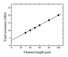
The three electrode systems such as transistors require more complicated methods, e.g. transmission line model, for the contact resistance approximation. The most common approach is the transmission line model (TLM). Here, the total device resistance is plotted as a function of the channel length:
where and are contact and channel resistancies, respectively, is the channel length/width, is gate insulator capacitance (per unit of area), is carrier mobility, and and are gate-source and drain-source voltages. Therefore, the linear extrapolation of total resistance to the zero channel length provides the contact resistance. The slope of the linear function is related to the channel transconductance and can be used for estimation of the â€contact resistance-free†carrier mobility. The approximations used here (linear potential drop across the channel region, constant contact resistance,...) lead sometimes to the channel dependent contact resistance.
Beside the TLM it was proposed the gated four-probe measurement and the modified time-of-flight method (TOF). The direct methods able to measure potential drop on the injection electrode directly are the Kelvin probe force microscopy (KFM) and the electric-field induced second harmonic generation.
Quantum limit

When a conductor has spatial dimensions close to , where is Fermi wavevector of the conducting material, Ohm's law does not hold anymore. These small devices are called quantum point contacts. Their conductance must be an integer multiple of the value , where is the electronic charge and is Planck's constant. Quantum point contacts behave more like waveguides than the classical wires of everyday life and may be described by the Landauer scattering formalism. Point-contact tunneling is an important technique for characterizing superconductors.
Other forms of contact resistance

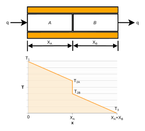
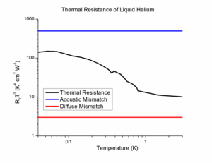
Measurements of thermal conductivity are also subject to contact resistance. Similarly, a drop in hydrostatic pressure (analogous to electrical voltage) occurs when fluid flow transitions from one channel to another.
Significance
Bad contacts are the cause of failure or poor performance in a wide variety of electrical devices. For example, corroded jumper cable clamps can frustrate attempts to start a vehicle that has a dead battery. Dirty or corroded contacts on a fuse or its holder can give the false impression that the fuse is blown. A sufficiently high contact resistance can cause substantial heating in a high current device. Unpredictable or noisy contacts are a major cause of the failure of electrical equipment.
Notes
- ^ W. Shockley, “Research and investigation of inverse epitaxial UHF power transistors,†Report No. A1-TOR-64-207, September 1964.
- ^ M. Weis, J. Lin, D. Taguchi, T. Manaka and M. Iwamoto (2010). "Insight into the contact resistance problem by direct probing of the potential drop in organic field-effect transistors". Appl. Phys. Lett. 97: 263304. Bibcode:2010ApPhL..97z3304W. doi:10.1063/1.3533020.Â
- ^ P.V. Pesavento, R.J. Chesterfield, C.R. Newman, C.D. Frisbie (2004). "Gated four-probe measurements on pentacene thin-film transistors: Contact resistance as a function of gate voltage and temperature". J. Appl. Phys. 96: 7312. Bibcode:2004JAP....96.7312P. doi:10.1063/1.1806533.Â
- ^ M. Weis, J. Lin, D. Taguchi, T. Manaka and M. Iwamoto (2009). "Analysis of Transient Currents in Organic Field Effect Transistor: The Time-of-Flight Method". J. Phys. Chem. C 113: 18459. doi:10.1021/jp908381b.Â
- ^ L. Bürgi, H. Sirringhaus, and R. H. Friend (2002). "Noncontact potentiometry of polymer field-effect transistors". Appl. Phys. Lett. 80: 2913. Bibcode:2002ApPhL..80.2913B. doi:10.1063/1.1470702.Â
- ^ M. Nakao, T. Manaka, M. Weis, E. Lim and M. Iwamoto (2009). "Probing carrier injection into pentacene field effect transistor by time-resolved microscopic optical second harmonic generation measurement". J. Appl. Phys. 106: 014511. Bibcode:2009JAP...106a4511N. doi:10.1063/1.3168434.Â
- ^ Landauer, Rolf (August 1976). "Spatial carrier density modulation effects in metallic conductivity". Physical Review B 14 (4): 1474â€"1479. Bibcode:1976PhRvB..14.1474L. doi:10.1103/PhysRevB.14.1474.Â


0 komentar :
Posting Komentar